


Introduction
The following questions and answers are drawn from the live audience Q&A during the SNIA Persistent Memory Special Interest Group webinar, New Memories for Inference and General-Purpose Compute. Moderated by PM SIG Chair Arthur Sainio, this session featured industry analysts Tom Coughlin and Jim Handy discussing new memory technologies, and the economic and scaling challenges shaping future compute systems.
This edited Q&A synthesizes responses from the webinar discussion to provide clear, concise insights for readers interested in persistent memory, chiplet architectures, and CXL-enabled systems.
Readers who would like to hear the full discussion and see the complete presentation can watch the on-demand webinar here.
Q: Really looking forward to these becoming commonplace. It has been a long wait, having been in HP memristor presentations in 2014.
A: That long wait reflects the reality of new memory technologies. While many concepts (such as memristors and phase-change memory) have been demonstrated for over a decade, their commercial success depends on manufacturability, yield, and volume. Today, the ecosystem is more mature: foundries support embedded MRAM and ReRAM, chiplet architectures are gaining traction, and standards like CXL are providing much greater architectural flexibility. These factors collectively make broader adoption more likely than in earlier cycles.
Q: Memory has a boom-bust cycle. Will these technologies behave any differently?
A: The memory market’s notorious boom-bust behavior applies only to the high-volume commodity memories: DRAM and NAND, where prices fluctuate dramatically. These new memories are not yet commodity products, so they do not exhibit the same cyclical pricing behavior.
If a new memory technology eventually displaces DRAM, it will likely inherit DRAM’s boom-bust behavior—but until then, adoption of stand-alone new memory chips will be driven more by architectural necessity than low prices.
Q: Why are MRAM and ReRAM not yet fully commercialized? What are the biggest hurdles in scaling and adoption? Which technologies require minimal application rewriting?
A: The primary hurdles are manufacturing scale and economics, not functionality. While MRAM and ReRAM offer compelling attributes (such as persistence, fast writes, and better scaling than SRAM), cost depends heavily on wafer volume and yield. Until volumes rise, pricing remains challenging.
From a software perspective, these memories can often be deployed with minimal application changes. For users who want to take advantage of these memories’ persistence, the SNIA Non-Volatile Memory Programming Model already provides a foundation for software support.
Q: What about Selector-Only Memory (SOM), Selector-Stacked Memory (SSM), and Single-chalcogenide X-point Memory (SXM)? Is there hope for these technologies?
A: These approaches resemble earlier phase-change memory concepts, including 3D XPoint. Their success will depend on whether they can achieve higher density and lower cost than competing technologies.
Designs based on 2-terminal selectors have an advantage because they can eliminate transistors, reducing cell size. However, success ultimately comes down to wafer volume. The technology that achieves the highest production scale will gain a cost advantage, while others may remain niche products.
Q: What are your thoughts on Google’s paper “A Case Against CXL Memory Pooling”? Will CXL still yield cost efficiencies?
A: Google argues that their sophisticated virtual machine placement eliminates any need for pooling. However, memory pooling is only one benefit of CXL.
CXL also enables:
- Mixing memory types (DRAM, MRAM, ReRAM, FRAM)
- Bridging DDR generations
- Disaggregated memory architectures
- Mesh networks
CXL acts as a bridge between DDR generations by decoupling the CPU’s fixed memory controller from the physical memory media. The most common example is that DDR4 RDIMMs are being reused today in DDR5 servers when they are put behind a CXL controller.
Even without pooling, CXL provides architectural flexibility and long-term design advantages. We don’t expect for CXL to be rejected solely on pooling arguments.
Q: Do these technologies rely heavily on rare-earth elements?
A: Some technologies, particularly MRAM, may use rare-earth elements (e.g., neodymium) in magnetic layers. However, these materials are used in extremely thin films, and the total material volume per device is small. Supply constraints are a consideration, but the scale is very different from applications like motors or large magnets.
Q: Will these new memories be produced in sufficient volume for hyperscalers without inflating consumer prices?
A: This is the classic chicken-and-egg problem. Prices fall only when volume increases, but volume increases only when prices are acceptable. This dynamic has limited the acceptance of technologies like Intel’s Optane despite its technical advantages.
Embedded applications are expected to drive early volume, followed by chiplets and discrete uses. As wafer volumes rise, economies of scale improve, opening broader markets. Until then, adoption will be limited rather than universal.
Q: If cost savings in embedded applications come from smaller die size and reduced SRAM, how does migrating to a specialized process not increase overall cost?
A: While specialized memory processes can be more expensive per wafer, total die cost is a function of both die area and per-wafer cost. SRAM consumes large die area and must be fabricated on the same advanced logic process—making it some of the most expensive memory in the system.
Replacing large on-die SRAM with an embedded new memory technology can reduce overall die size dramatically—often cutting total chip cost by more than 50%. This die size savings can offset any increase in wafer processing cost.
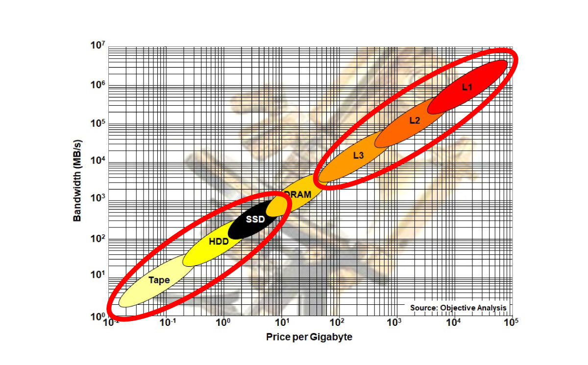
Q: SRAM scaling has stalled below 5 nm, while MRAM is not widely available below 7 nm. How does this strategy work in practice?
A: Foundries often introduce a new memory technology after logic processes mature, and memory layers can use different lithographic tuning than logic.
MRAM is already available at 22 nm and 16 nm, with roadmaps extending to 8 nm and 5 nm for specific applications. Furthermore, memory and logic do not need to scale together – some of today’s processors already team a tight logic process with a looser memory process.
There are several options for applications that need a cost-effective SRAM substitute at a tight process geometry. These include:
- Using a new memory technology in chiplet form, which separates logic and memory processes for optimal cost and yield
- Deploying larger, slower persistent on-chip caches, made using a new memory technology, to augment a smaller size of high-speed SRAM
This flexibility enables continued system scaling even as SRAM density plateaus.
Closing Thoughts
As volumes grow and costs decline, persistent memories are increasingly positioned to reshape compute architectures rather than simply replace existing memory types. While no single new memory technology is guaranteed to win, it is clear that established memories are on the verge of being replaced by alternatives that will scale with future logic processes to improve costs while providing persistence, faster writes, and lower power to both AI and general-purpose computing.
Readers who would like to learn more about the research discussed during our webinar can visit Objective Analysis and Coughlin Associates websites.
Leave a Reply