


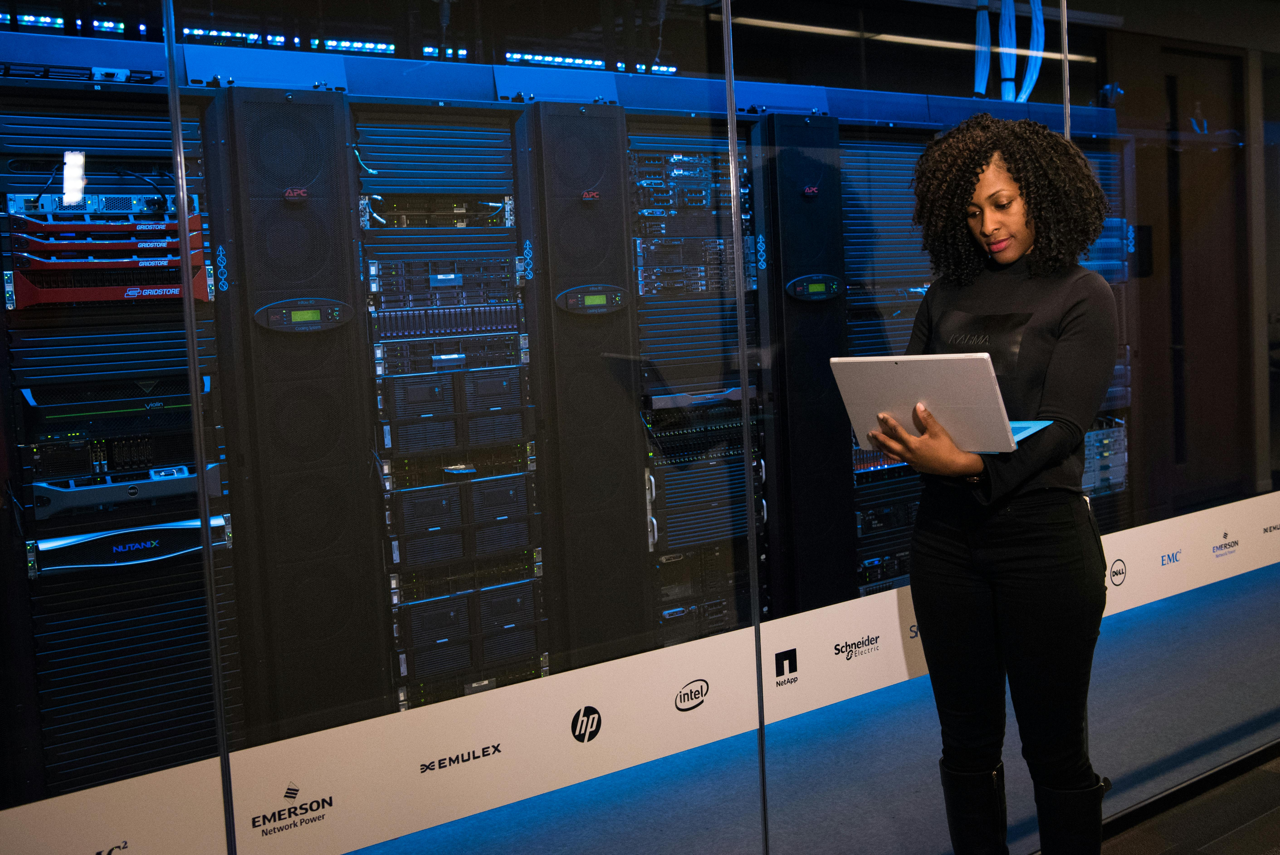

Measuring power efficiency in datacenter storage is a complex endeavor. A number of factors play a role in assessing individual storage devices or system-level logical storage for power efficiency. Luckily, our SNIA experts make the measuring easier!
In this SNIA Experts on Data blog series, our experts in the SNIA Solid State Storage Technical Work Group and the SNIA Green Storage Initiative explore factors to consider in power efficiency measurement, including the nature of application workloads, IO streams, and access patterns; the choice of storage products (SSDs, HDDs, cloud storage, and more); the impact of hardware and software components (host bus adapters, drivers, OS layers); and access to read and write caches, CPU and GPU usage, and DRAM utilization.
Join us on our journey to better power efficiency as we continue with Part 3: Traditional Differences in Power Consumption: Hard Disk Drives vs Solid State Drives. And if you missed our earlier segments, click on the titles to read them: Part 1: Key Issues in Power Efficiency Measurement, and Part 2: Impact of Workloads on Power Efficiency Measurement.. Bookmark this blog and check back in April for the final installment of our four-part series. And explore the topic further in the SNIA Green Storage Knowledge Center.
Traditional Differences in Power Consumption: Hard Disk Drives vs Solid State Drives
There are significant differences in power efficiency between Hard Disk Drives (HDDs) and Solid State Drives (SSDs). While some commentators have examined differences in power efficiency measurement for HDDs v SSDs, much of the analysis has not accounted for the key power efficiency contributing factors outlined in this blog.
As a simple generalization at the individual storage device level, HDDs show higher power consumption than SSDs. In addition, SSDs have higher performance (IOPS and MB/s) often by an order of magnitude or more. Hence, cursory consideration of device power efficiency measurement, expressed as IOPS/W or MB/s/W, will typically favor the faster SSD with lower device power consumption.
On the other hand, depending on the workload and IO transfer size, HDD devices and systems may exhibit better IOPS/W and MB/s/W if measured to large block sequential RW workloads where head actuators can reside on the disk OD (outer diameter) with limited seek accesses.
The above traditional HDD and SSD power efficiency considerations can be described at the device level as involving the following key points:
HDDs (Hard Disk Drives):
- Mechanical Components: HDDs consist of spinning disks and mechanical read/write heads. These moving parts consume a substantial amount of power, especially during startup and when seeking data.
- Idle Power Consumption: Even when not actively reading or writing data, HDDs still consume a notable amount of power to keep the disks spinning and ready to access data
- Access Time Impact: The mechanical nature of HDDs leads to longer access times compared to SSDs. This means the drive remains active for longer periods during data access, contributing to higher power consumption.
- No Moving Parts: SSDs are entirely electronic and have no moving parts. As a result, they consume less power during both idle and active states compared to HDDs
- Faster Access Times: SSDs have much faster access times since there are no mechanical delays. This results in quicker data retrieval and reduced active time, contributing to lower power consumption
- Energy Efficiency: SSDs are generally more energy-efficient, as they consume less power during read and write operations. This is especially noticeable in laptops and portable devices, where battery life is critical
- Less Heat Generation: Due to their lack of moving parts, SSDs generate less heat during operation, which can lead to better thermal efficiency in systems.


 , though, that shouldn’t be that much of a problem since it’s a transactional protocol. The reads, then, will probably rival DRAM speeds for MRAM and for resistive RAM (MRAM might get up to DRAM speeds with its writes too). In fact, there are technologies like spin-orbit torque and even voltage-controlled magnetic anisotropy that promise higher performance and also low write latency for MRAM technologies. I think that probably most applications are read intensive and so the read is the real place where the focus is, but it does look like we are going to get there.
Q: Are all the new Memory technology protocols (electrically) compatible to DRAM interfaces like DDR4 or DDR5? If not, then shouldn’t those technologies have lower chances of adoption as they add dependency on custom in-memory controller?
A: That’s just a logic problem. There’s nothing innate about any memory technology that couples it tightly with any kind of a bus, and so because NOR Flash and SRAM are the easy targets so far, most emerging technologies have used a NOR flash or SRAM type interface. However, in the future they could use DDR. There’re some special twists because you don’t have to refresh emerging memory technologies. but you know in general they could use DDR.
But one of the beauties of CXL is that you put anything you want to with any kind of interface on the other side of CXL and CXL erases what the differences are. It moderates them so although they may have different performances it’s hidden behind the CXL network. Then the burden goes on to the CXL controller designers to make sure that those emerging technologies, whether it’s MRAM or others, can be adopted behind that CXL protocol. My expectation is for there to be a few companies early on who provide CXL controllers that that do have some kind of a specialty interface on them whether it’s for MRAM or for Resistive RAM or something like that, and then eventually for them to move their way into the mainstream. Another interesting thing about CXL is that we may even see a hierarchy of different memories within CXL itself which also includes as part of CXL including domain specific processors or accelerators that operate close to memory, and so there are very interesting opportunities there as well. If you can do processing close to memory you lower the amount of data you’re moving around and you’re saving a lot of power for the computing system.
Q: Emerging memory technologies have a byte-level direct access programming model, which is in contrast to block-based NAND Flash. Do you think this new programming model will eventually replace NAND Flash as it reduces the overhead and reduces the power of transferring Data?
A: It’s a question of cost and that’s something that was discussed very much in our webinar. If you haven’t got a cost that’s comparable to NAND Flash, then you can’t really displace it. But as far as the interface is concerned, the NAND interface is incredibly clumsy. All of these technologies do have both byte interfaces rather than a block interface but also, they can write in place – they don’t need to have a pre-erased block to write into. That from a technical standpoint is a huge advantage and now it’s just a question of whether or not they can get the cost down – which means getting the volume up.
Q: Can you discuss the High Bandwidth Memory (HBM) trends? What about memories used with Graphic Processing Units (GPUs)?
A: That topic isn’t the subject of this webinar as this webinar is about emerging memory technologies. But, to comment, we don’t expect to see emerging memory technologies adopt an HBM interface anytime in the really near future because HBM does springboard off DRAM and, as we discussed on one of the slides, DRAM has a transition that we don’t know when it’s going to happen that it goes to another emerging memory technology. We’ve put it into the early 2030s in our chart, but it could be much later than that and HBM won’t convert over to an emerging memory technology until long after that.
However, HBM involves stacking of chips and that ultimately could happen. It’s a more expensive process right now – a way of getting a lot of memory very close to a processor – and if you look at some of the NVIDIA applications for example, this is an example of the Chiplet technology and HBM can play a role in those Chiplet technologies for GPUs.. That’s another area that’s going to be using emerging memories as well – in the Chiplets. While we didn’t talk about that so much in this webinar, it is another place for emerging memories to be playing a role.
There’s one other advantage to using an emerging memory that we did not talk about: emerging memories don’t need refresh. As a matter of fact, none of the emerging memory technologies need refresh. More power is consumed by DRAM refreshing than by actual data accesses. And so, if you can cut that out of it, you might be able to stack more chips on top of each other and get even more performance, but we still wouldn’t see that as a reason for DRAM to be displaced early on in HBM and then later on in the mainstream DRAM market. Although, if you’re doing all those refreshes there’s a fair amount of potential of heat generation by doing that, which may have packaging implications as well. So, there may be some niche areas in there which could be some of the first ways in which some of these emerging memories are potentially used for those kinds of applications, if the performance is good enough.
Q: Why have some memory companies failed? Apart from the cost/speed considerations you mention, what are the other minimum envelope features that a new emerging memory should have? Is capacity (I heard 32Gbit multiple times) one of those criteria?
A: Shipping a product is probably the single most important activity for success. Companies don’t have to make a discrete or standalone SRAM or emerging memory chip but what they need to do is have their technology be adopted by somebody who is shipping something if they’re not going to ship it themselves. That’s what we see in the embedded market as a good path for emerging memory IP: To get used and to build up volume. And as the volume and comfort with manufacturing those memories increase, it opens up the possibility down the road of lower costs with higher volume standalone memory as well.
Q: What are the trends in DRAM interfaces? Would you discuss CXL’s role in enabling composable systems with DRAM pooling?
A: CXL, especially CXL 3.0, has particularly pointed at pooling. Pooling is going to be an extremely important development in memory with CXL, and it’s one of the reasons why CXL probably will proliferate. It allows you to be able to allocate memory which is not attached to particular server CPUs and therefore to make more efficient and effective use of those memories. We mentioned this earlier when we said that right now DRAM is that memory with some NAND Flash products out there too. But this could expand into other memory technologies behind CXL within the CXL pool as well as accelerators (domain specific processors) that do some operations closer to where the memory lives. So, we think there’s a lot of possibilities in that pooling for the development and growth of emerging memories as well as conventional memories.
Q: Do you think molecular-based technologies (DNA or others) can emerge in the coming years as an alternative to some of the semiconductor-based memories?
A: DNA and other memory technologies are in a relatively early stage but there are people who are making fairly aggressive plans on what they can do with those technologies. We think the initial market for those molecular memories are not in this high performance memory application; but especially with DNA, the potential density of storage and the fact that you can make lots of copies of content by using genetic genomic processes makes them very attractive potentially for archiving applications. The things we’ve seen are mostly in those areas because of the performance characteristics. But the potential density that they’re looking at is actually aimed at that lower part of the market, so it has to be very, very cost effective to be able to do that, but the possibilities are there. But again, as with the emerging high performance memories, you still have the economies of scale you have to deal with – if you can’t scale it fast enough the cost won’t go down enough that will actually will be able to compete in those areas. So it faces somewhat similar challenges, though in a different part of the market.
Earlier in the webcast, we said when showing the orb chart, that for something to fit into the computing storage hierarchy it has to be cheaper than the next faster technology and faster than the next cheaper technology. DNA is not a very fast technology and so that automatically says it has to be really cheap for it to catch on and that puts it in a very different realm than the emerging memories that we’re talking about here. On the other hand, you never know what someone’s going to discover, but right now the industry doesn’t know how to make fast molecular memories.
Q: What is your intuition on how tomorrow’s highly dense memories might impact non-load/store processing elements such as AI accelerators? As model sizes continue to grow and energy density becomes more of an issue, it would seem like emerging memories could thrive in this type of environment. Your thoughts?
A: Any memory would thrive in an environment where there was an unbridled thirst for memory. as artificial intelligence (AI) currently is. But AI is undergoing some pretty rapid changes, not only in the number of the parameters that are examined, but also in the models that are being used for it. We recently read a paper that was written by Apple* where they actually found ways of winnowing down the data that was used for a large language model into something that would fit into an Apple MacBook Pro M2 and they were able to get good performance by doing that. They really accelerated things by ignoring data that didn’t really make any difference. So, if you take that kind of an approach and say: “Okay. If those guys keep working on that problem that way, and they take it to the extreme, then you might not need all that much memory after all.” But still, if memory were free, I’m sure that there’d be a ton of it out there and that is just a question of whether or not these memories can get cheaper than DRAM so that they can look like they’re free compared to what things look like today.
There are three interesting elements of this: First, CXL, in addition allowing mixing of memory types, again allows you to put in those domain specific processors as well close to the memory. Perhaps those can do some of the processing that’s part of the model, in which case it would lower the energy consumption. The other thing it supports is different computing models than what we traditionally use. Of course there is quantum computing, but there also is something called neural networks which actually use the memory as a matrix multiplier, and those are using these emerging memories for that technology which could be used for AI applications. The other thing that’s sort of hidden behind this is that spin tunnelling is changing processing itself in that right now everything is current-based, but there’s work going on in spintronic based devices that instead of using current would use the spin of electrons for moving data around, in which case we can avoid resistive heating and our processing could run a lot cooler and use less energy to do so. So, there’s a lot of interesting things that are kind of buried in the different technologies being used for these emerging memories that actually could have even greater implications on the development of computing beyond just the memory application themselves. And to elaborate on spintronics, we’re talking about logic and not about spin memory – using spins rather than that of charge which is current.
Q: Flash has an endurance issue (maximum number of writes before it fails). In your opinion, what is the minimum acceptable endurance (number of writes) that an emerging memory should support?
It’s amazing how many techniques have fallen into place since wear was an issue in flash SSDs. Today’s software understands which loads have high write levels and which don’t, and different SSDs can be used to handle the two different kinds of load. On the SSD side, flash endurance has continually degraded with the adoption of MLC, TLC, and QLC, and is sometimes measured in the hundreds of cycles. What this implies is that any emerging memory can get by with an equally low endurance as long as it’s put behind the right controller.
In high-speed environments this isn’t a solution, though, since controllers add latency, so “Near Memory” (the memory tied directly to the processor’s memory bus) will need to have higher endurance. Still, an area that can help to accommodate that is the practice of putting code into memories that have low endurance and data into higher-endurance memory (which today would be DRAM). Since emerging memories can provide more bits at a lower cost and power than DRAM, the write load to the code space should be lower, since pages will be swapped in and out more frequently. The endurance requirements will depend on this swapping, and I would guess that the lowest-acceptable level would be in the tens of thousands of cycles.
Q: It seems that persistent memory is more of an enterprise benefit rather than a consumer benefit. And consumer acceptance helps the advancement and cost scaling issues. Do you agree? I use SSDs as an example. Once consumers started using them, the advancement and prices came down greatly.
Anything that drives increased volume will help. In most cases any change to large-scale computing works its way down to the PC, so this should happen in time here, too. But today there’s a growing amount of MRAM use in personal fitness monitors, and this will help drive costs down, so initial demand will not exclusively come from enterprise computing. At the same time, the IBM FlashDrive that we mentioned uses MRAM, too, so both enterprise and consumer are already working to simultaneously grow consumption.
Q: The CXL diagram (slide 22 in the
, though, that shouldn’t be that much of a problem since it’s a transactional protocol. The reads, then, will probably rival DRAM speeds for MRAM and for resistive RAM (MRAM might get up to DRAM speeds with its writes too). In fact, there are technologies like spin-orbit torque and even voltage-controlled magnetic anisotropy that promise higher performance and also low write latency for MRAM technologies. I think that probably most applications are read intensive and so the read is the real place where the focus is, but it does look like we are going to get there.
Q: Are all the new Memory technology protocols (electrically) compatible to DRAM interfaces like DDR4 or DDR5? If not, then shouldn’t those technologies have lower chances of adoption as they add dependency on custom in-memory controller?
A: That’s just a logic problem. There’s nothing innate about any memory technology that couples it tightly with any kind of a bus, and so because NOR Flash and SRAM are the easy targets so far, most emerging technologies have used a NOR flash or SRAM type interface. However, in the future they could use DDR. There’re some special twists because you don’t have to refresh emerging memory technologies. but you know in general they could use DDR.
But one of the beauties of CXL is that you put anything you want to with any kind of interface on the other side of CXL and CXL erases what the differences are. It moderates them so although they may have different performances it’s hidden behind the CXL network. Then the burden goes on to the CXL controller designers to make sure that those emerging technologies, whether it’s MRAM or others, can be adopted behind that CXL protocol. My expectation is for there to be a few companies early on who provide CXL controllers that that do have some kind of a specialty interface on them whether it’s for MRAM or for Resistive RAM or something like that, and then eventually for them to move their way into the mainstream. Another interesting thing about CXL is that we may even see a hierarchy of different memories within CXL itself which also includes as part of CXL including domain specific processors or accelerators that operate close to memory, and so there are very interesting opportunities there as well. If you can do processing close to memory you lower the amount of data you’re moving around and you’re saving a lot of power for the computing system.
Q: Emerging memory technologies have a byte-level direct access programming model, which is in contrast to block-based NAND Flash. Do you think this new programming model will eventually replace NAND Flash as it reduces the overhead and reduces the power of transferring Data?
A: It’s a question of cost and that’s something that was discussed very much in our webinar. If you haven’t got a cost that’s comparable to NAND Flash, then you can’t really displace it. But as far as the interface is concerned, the NAND interface is incredibly clumsy. All of these technologies do have both byte interfaces rather than a block interface but also, they can write in place – they don’t need to have a pre-erased block to write into. That from a technical standpoint is a huge advantage and now it’s just a question of whether or not they can get the cost down – which means getting the volume up.
Q: Can you discuss the High Bandwidth Memory (HBM) trends? What about memories used with Graphic Processing Units (GPUs)?
A: That topic isn’t the subject of this webinar as this webinar is about emerging memory technologies. But, to comment, we don’t expect to see emerging memory technologies adopt an HBM interface anytime in the really near future because HBM does springboard off DRAM and, as we discussed on one of the slides, DRAM has a transition that we don’t know when it’s going to happen that it goes to another emerging memory technology. We’ve put it into the early 2030s in our chart, but it could be much later than that and HBM won’t convert over to an emerging memory technology until long after that.
However, HBM involves stacking of chips and that ultimately could happen. It’s a more expensive process right now – a way of getting a lot of memory very close to a processor – and if you look at some of the NVIDIA applications for example, this is an example of the Chiplet technology and HBM can play a role in those Chiplet technologies for GPUs.. That’s another area that’s going to be using emerging memories as well – in the Chiplets. While we didn’t talk about that so much in this webinar, it is another place for emerging memories to be playing a role.
There’s one other advantage to using an emerging memory that we did not talk about: emerging memories don’t need refresh. As a matter of fact, none of the emerging memory technologies need refresh. More power is consumed by DRAM refreshing than by actual data accesses. And so, if you can cut that out of it, you might be able to stack more chips on top of each other and get even more performance, but we still wouldn’t see that as a reason for DRAM to be displaced early on in HBM and then later on in the mainstream DRAM market. Although, if you’re doing all those refreshes there’s a fair amount of potential of heat generation by doing that, which may have packaging implications as well. So, there may be some niche areas in there which could be some of the first ways in which some of these emerging memories are potentially used for those kinds of applications, if the performance is good enough.
Q: Why have some memory companies failed? Apart from the cost/speed considerations you mention, what are the other minimum envelope features that a new emerging memory should have? Is capacity (I heard 32Gbit multiple times) one of those criteria?
A: Shipping a product is probably the single most important activity for success. Companies don’t have to make a discrete or standalone SRAM or emerging memory chip but what they need to do is have their technology be adopted by somebody who is shipping something if they’re not going to ship it themselves. That’s what we see in the embedded market as a good path for emerging memory IP: To get used and to build up volume. And as the volume and comfort with manufacturing those memories increase, it opens up the possibility down the road of lower costs with higher volume standalone memory as well.
Q: What are the trends in DRAM interfaces? Would you discuss CXL’s role in enabling composable systems with DRAM pooling?
A: CXL, especially CXL 3.0, has particularly pointed at pooling. Pooling is going to be an extremely important development in memory with CXL, and it’s one of the reasons why CXL probably will proliferate. It allows you to be able to allocate memory which is not attached to particular server CPUs and therefore to make more efficient and effective use of those memories. We mentioned this earlier when we said that right now DRAM is that memory with some NAND Flash products out there too. But this could expand into other memory technologies behind CXL within the CXL pool as well as accelerators (domain specific processors) that do some operations closer to where the memory lives. So, we think there’s a lot of possibilities in that pooling for the development and growth of emerging memories as well as conventional memories.
Q: Do you think molecular-based technologies (DNA or others) can emerge in the coming years as an alternative to some of the semiconductor-based memories?
A: DNA and other memory technologies are in a relatively early stage but there are people who are making fairly aggressive plans on what they can do with those technologies. We think the initial market for those molecular memories are not in this high performance memory application; but especially with DNA, the potential density of storage and the fact that you can make lots of copies of content by using genetic genomic processes makes them very attractive potentially for archiving applications. The things we’ve seen are mostly in those areas because of the performance characteristics. But the potential density that they’re looking at is actually aimed at that lower part of the market, so it has to be very, very cost effective to be able to do that, but the possibilities are there. But again, as with the emerging high performance memories, you still have the economies of scale you have to deal with – if you can’t scale it fast enough the cost won’t go down enough that will actually will be able to compete in those areas. So it faces somewhat similar challenges, though in a different part of the market.
Earlier in the webcast, we said when showing the orb chart, that for something to fit into the computing storage hierarchy it has to be cheaper than the next faster technology and faster than the next cheaper technology. DNA is not a very fast technology and so that automatically says it has to be really cheap for it to catch on and that puts it in a very different realm than the emerging memories that we’re talking about here. On the other hand, you never know what someone’s going to discover, but right now the industry doesn’t know how to make fast molecular memories.
Q: What is your intuition on how tomorrow’s highly dense memories might impact non-load/store processing elements such as AI accelerators? As model sizes continue to grow and energy density becomes more of an issue, it would seem like emerging memories could thrive in this type of environment. Your thoughts?
A: Any memory would thrive in an environment where there was an unbridled thirst for memory. as artificial intelligence (AI) currently is. But AI is undergoing some pretty rapid changes, not only in the number of the parameters that are examined, but also in the models that are being used for it. We recently read a paper that was written by Apple* where they actually found ways of winnowing down the data that was used for a large language model into something that would fit into an Apple MacBook Pro M2 and they were able to get good performance by doing that. They really accelerated things by ignoring data that didn’t really make any difference. So, if you take that kind of an approach and say: “Okay. If those guys keep working on that problem that way, and they take it to the extreme, then you might not need all that much memory after all.” But still, if memory were free, I’m sure that there’d be a ton of it out there and that is just a question of whether or not these memories can get cheaper than DRAM so that they can look like they’re free compared to what things look like today.
There are three interesting elements of this: First, CXL, in addition allowing mixing of memory types, again allows you to put in those domain specific processors as well close to the memory. Perhaps those can do some of the processing that’s part of the model, in which case it would lower the energy consumption. The other thing it supports is different computing models than what we traditionally use. Of course there is quantum computing, but there also is something called neural networks which actually use the memory as a matrix multiplier, and those are using these emerging memories for that technology which could be used for AI applications. The other thing that’s sort of hidden behind this is that spin tunnelling is changing processing itself in that right now everything is current-based, but there’s work going on in spintronic based devices that instead of using current would use the spin of electrons for moving data around, in which case we can avoid resistive heating and our processing could run a lot cooler and use less energy to do so. So, there’s a lot of interesting things that are kind of buried in the different technologies being used for these emerging memories that actually could have even greater implications on the development of computing beyond just the memory application themselves. And to elaborate on spintronics, we’re talking about logic and not about spin memory – using spins rather than that of charge which is current.
Q: Flash has an endurance issue (maximum number of writes before it fails). In your opinion, what is the minimum acceptable endurance (number of writes) that an emerging memory should support?
It’s amazing how many techniques have fallen into place since wear was an issue in flash SSDs. Today’s software understands which loads have high write levels and which don’t, and different SSDs can be used to handle the two different kinds of load. On the SSD side, flash endurance has continually degraded with the adoption of MLC, TLC, and QLC, and is sometimes measured in the hundreds of cycles. What this implies is that any emerging memory can get by with an equally low endurance as long as it’s put behind the right controller.
In high-speed environments this isn’t a solution, though, since controllers add latency, so “Near Memory” (the memory tied directly to the processor’s memory bus) will need to have higher endurance. Still, an area that can help to accommodate that is the practice of putting code into memories that have low endurance and data into higher-endurance memory (which today would be DRAM). Since emerging memories can provide more bits at a lower cost and power than DRAM, the write load to the code space should be lower, since pages will be swapped in and out more frequently. The endurance requirements will depend on this swapping, and I would guess that the lowest-acceptable level would be in the tens of thousands of cycles.
Q: It seems that persistent memory is more of an enterprise benefit rather than a consumer benefit. And consumer acceptance helps the advancement and cost scaling issues. Do you agree? I use SSDs as an example. Once consumers started using them, the advancement and prices came down greatly.
Anything that drives increased volume will help. In most cases any change to large-scale computing works its way down to the PC, so this should happen in time here, too. But today there’s a growing amount of MRAM use in personal fitness monitors, and this will help drive costs down, so initial demand will not exclusively come from enterprise computing. At the same time, the IBM FlashDrive that we mentioned uses MRAM, too, so both enterprise and consumer are already working to simultaneously grow consumption.
Q: The CXL diagram (slide 22 in the 

Leave a Reply